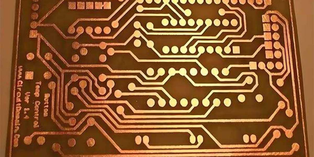
Introduction
Surface treatment in PCB (Printed Circuit Board) manufacturing is a crucial step, with two primary functions: protecting the exposed copper circuitry and providing a good solderable surface for assembly. As the electronics industry continues to evolve, so do the technologies for PCB surface treatments. Each method offers specific advantages tailored to different applications, making the correct choice critical for both performance and cost efficiency.
Common PCB Surface Treatment Techniques
1. Hot Air Solder Leveling (HASL)
Principle: HASL involves applying molten solder (tin-lead alloy) onto the PCB surface, which is then leveled with hot compressed air to form a protective, solderable coating that resists copper oxidation.
Advantages: Cost-effective.
Disadvantages: Uneven pad surfaces and poor coplanarity, making it unsuitable for fine-pitch components. Lead-containing HASL is harmful to the environment.
2. Organic Solderability Preservatives (OSP)
Principle: OSP forms a thin, protective organic film on the bare copper surface via chemical treatment, preventing oxidation while preserving the solderability of the copper pads.
Advantages: Environmentally friendly, no lead contamination.
Disadvantages: Difficult to inspect as OSP is transparent and colorless. Non-conductive, which can affect electrical testing. Requires stronger flux during soldering and cannot be stored for long periods.
3. Electroless Nickel Immersion Gold (ENIG)
Principle: ENIG deposits a layer of nickel and a thin layer of gold on the copper surface via a chemical process. The nickel acts as a diffusion barrier, while the gold prevents the oxidation of nickel.
Advantages: Excellent flatness and solderability, ideal for contact surfaces like keypads.
Disadvantages: Complex process with stringent control requirements. Prone to the “black pad” phenomenon, compromising solder joint reliability.
4. Electroless Nickel Electroless Palladium Immersion Gold (ENEPIG)
Principle: ENEPIG introduces a palladium layer between nickel and gold, offering additional protection against corrosion.
Advantages: Superior corrosion resistance, a viable alternative to ENIG.
Disadvantages: Expensive due to the high cost of palladium, which is a scarce resource.
Requires precise control similar to ENIG.
5. Immersion Silver
Principle: In this method, silver is deposited onto the PCB surface, forming a thin protective film that enhances solderability.
Advantages: Excellent flatness and solderability.
Disadvantages: Risk of silver migration, especially in humid environments.
6. Immersion Tin
Principle: Immersion tin provides a uniform, flat surface by depositing tin onto the PCB.
Advantages: Flat surface with no lead content.
Disadvantages: Short lifespan, especially under high temperature and humidity conditions.
Conclusion
Each surface treatment technique offers distinct advantages and limitations. Selecting the appropriate method depends on factors like cost, environmental considerations, application requirements, and performance expectations. As the electronics industry demands higher density, reliability, and sustainability, PCB surface treatment technologies will continue to evolve, providing better solutions for advanced applications. Gekunflex delivers high-quality Flexible PCB board services to fulfill your order requirements with excellence.


